Goal: Build a voice recorder that records and plays back 8-bit digital audio samples. Implement a low-pass FIR filter module that can be used as an anti-aliasing and reconstruction filter.
Useful links
Checkoff List
Please be ready with the following when checking off Lab #4:
During checkoff you may be asked to discuss one or more of the following questions:
When you're done remember to upload your Verilog files to the course website so that they can be reviewed.
Digital Audio Interface
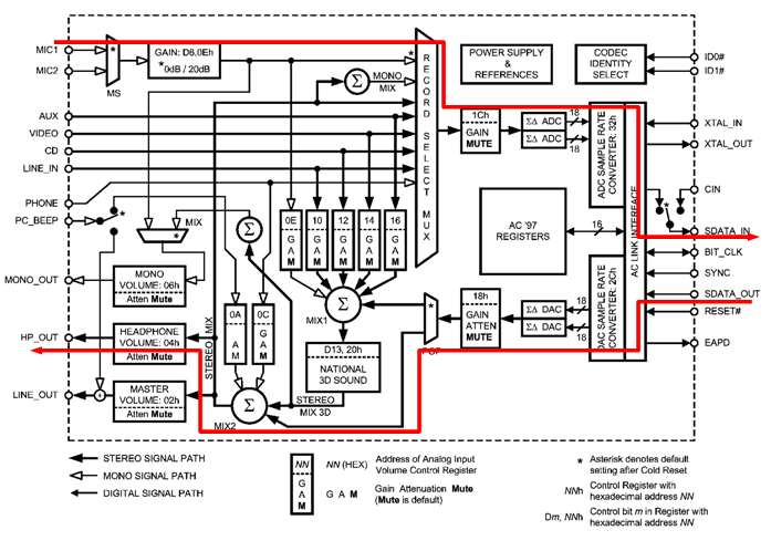
Our labkit is equipped with an AC97 Audio Codec chip (a National Semiconductor LM4550) which serves as an interface between the analog world of traditional audio components (e.g., headphones and microphones) and the digital world of the FPGA. The block diagram of the LM4550 shown below has been marked up to show the processing paths we'll be using for this lab:
Incoming audio from microphone (top arrow, pointing left-to-right): the incoming audio signal from the microphone is boosted by +20dB by an on-chip amplifier and then selected as the input source for the two (one for each of the stereo channels) 18-bit sigma- delta analog-to-digital converters (ΣΔADCs). The ADCs sample the analog waveforms at 48kHz, digitize the sampled voltages, and output sequences of 18-bit two's complement numbers (referred to as the pulse-code modulated or PCM data). Each pair (left and right channel) of PCM samples is packaged along with other status data into a 256-bit frame which is then transmitted serially at 12.288Mhz (= 256 * 48Khz) to the FPGA via the SDATA-IN pin.
Outgoing audio to headphones (bottom arrow, pointing right-to-left): the FPGA transmits a 256-bit frame of serial data to the AC97 chip via the SDATA-OUT pin. Each frame contains two 18-bit fields with PCM data for the left and right audio channels. The PCM data is converted to two 48kHz analog waveforms by the sigma-delta digital-to- analog converters (ΣΔDACs). The analog waveforms are amplified and sent to the stereo headphones.
So 48,000 times per second the AC97 codec provides two stereo PCM samples from the microphone and accepts two stereo PCM samples for the headphones. (Actually the microphone is a monaural source and so the same data appears on both the left and right incoming data streams.) It's the FPGA's job to keep up with the codec's data rates since the codec does not have on-chip buffering for either the incoming or outgoing data streams.
Voice recorder
The goal of this lab is to implement a voice recorder using the labkit's AC97 codec and FPGA. The top-level plan is pretty simple -- when recording, store the stream of incoming samples in a memory, when playing back feed the stored data stream back to the codec.
There are (of course) some interesting details:
Remembering about Nyquist rates, the original 48kHz data represents audio frequencies up to 24kHz. Down-sampling to 6kHz yields data that represents audio frequencies up to 3kHz. In order to prevent aliasing during the down-sampling process we'll need to remove audio frequencies between 3kHz and 24kHz from the data before down-sampling by passing the incoming samples through a low-pass anti-aliasing filter.
But if we do that we will hear 6kHz noise (and its overtones) introduced by by the replication process. So we'll pass the outgoing samples through a low-pass reconstruction filter to ensure that the 48kHz output stream only contains audio frequencies up to 3kHz.
In fact we can use the same low-pass filter as both an anti-aliasing filter during recording and a reconstruction filter during playback.
Step 0: Getting started with lab4.v
Download lab4.v by clicking right on the link and selecting "Save As". This file contains several Verilog modules:
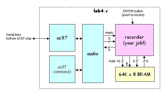
lab4: a modified version of labkit.v that includes instances of the audio and recorder modules, hooking them up appropriately to each other and the pins connecting to the AC97 codec. The labkit's ENTER pushbutton is used as the record/playback button (push to record). You shouldn't need to modify this module.
debounce: used to debounce and synchronize pushbuttons.
audio: a wrapper around the ac97 and ac97commands modules which implement the low-level interface to codec. This module has three ports of interest to us: a ready output that signals users of this module that a new sample is ready, and two 8-bit data ports, one for incoming monaural PCM data and one for outgoing monaural PCM data. You shouldn't need to modify this module.
ac97: interfaces with the AC97 codec, transmitting and receiving the 256-bit serial data streams. It has ports for both incoming and outgoing 18-bit stereo PCM data. You shouldn't need to modify this module.
ac97commands: generates a repeating sequence of writes to the AC97 command registers that perform the appropriate initialization. In this case, that includes selecting the microphone as the input source, setting the correct amplifier gains, etc. You shouldn't need to modify this module.
tone750hz: supplies a 20-bit PCM stream which if played at 48kHz produces a 750Hz sinewave. You shouldn't need to modify this module.
mybram: a Verilog module that allows you to quickly create FPGA memories based on BRAMs. See the discussion in Step 1 below.
fir31: a dummy module serving as a placeholder for the 31-tap low-pass FIR filter that you'll design.
coeffs31: a combinational module that returns a signed 10-bit filter coefficient given a tap number between 0 and 30. The coefficients were determined by using the fir1(30,.125) command in Matlab, then scaling the result by 2**10 to produce integer tap coefficients.
recorder: You'll be modifying this module to implement the necessary functionality. The supplied module tests the basic functionality of the microphone and headphones. In playback mode, this dummy module sends a 750Hz tone to the headphones. In record mode, it loops incoming samples back to the outgoing data stream, so you should hear your voice in the headphones. The module has the following ports all of which are synchronous with clock_27mhz:
| clock_27mhz | input | system clock |
| reset | input | 1 to reset the module to its initial state |
| playback | input | 1 for playback, 0 for record |
| filter | input | 1 for filtering, 0 for no filtering |
| ready | input | transitions from 0 to 1 when a new sample is available |
| from_ac97_data[7:0] | input | 8-bit PCM data from the microphone (signed, two's complement) |
| to_ac97_data[7:0] | output | 8-bit PCM data to the headphones (signed, two's complement) |
Using the Xilinx tools, build a lab4 project, compile lab4.v and load lab4.bit into the labkit. Plug in the headphone and microphone plugs from the headset into the appropriate jacks on the left-hand side of the labkit. You should hear a 750Hz tone in the headset. Pushing the ENTER pushbutton should silence the tone and instead you should hear sounds picked up by the microphone.
You can adjust the volume of the playback by pressing the UP and DOWN buttons (the top and bottom buttons in the diamond group of buttons to the left of the ENTER button). Each press will change the volume by 1 step over the range of 32 steps. During playback the current volume is displayed in the low-order 5 bits of the LEDs. The initial volume is low, so press the up button multiple times until you can hear the playback tone comfortably.
Step 1: Implement the basic recording without filtering
You can build your 64Kx8 memory using the ISE tool's Architectural Wizard as outlined in lecture. This takes a while, so you may find it easier to use the mybram module included in lab4.v. In general, unless you need to load a memory with known values, making the appropriately parameterized instance of mybram will take less of your valuable design time!
module mybram #(parameter LOGSIZE=14, WIDTH=1)
              (input wire [LOGSIZE-1:0] addr,
               input wire clk,
               input wire [WIDTH-1:0] din,
               output reg [WIDTH-1:0] dout,
               input wire we);
   // let the tools infer the right number of BRAMs
   (* ram_style = "block" *)
   reg [WIDTH-1:0] mem[(1<<LOGSIZE)-1:0];
   always @(posedge clk) begin
     if (we) mem[addr] <= din;
     dout <= mem[addr];
   end
endmodule

// example use: make a 64K x 8 memory
mybram #(.LOGSIZE(16),.WIDTH(8))
       example(.addr(a),.clk(clock),.we(we),.din(mem_in),.dout(mem_out));
Record mode: When entering record mode, reset the memory address. When the ready input is asserted, a new sample from the microphone is available on the from_ac97_data[7:0] inputs at the rising edge of clock_27mhz. Store every eighth sample in the memory, incrementing the memory address after each write. You should also keep track of the highest memory address that's written. If you fill up memory, you should stop recording new samples.
Playback mode: When entering playback mode, reset the memory address. When the ready input is asserted, supply a 8-bit sample on the to_ac97_data[7:0] outputs and hold it there until the next sample is requested. For now, read a new sample from the memory every eight transitions of ready and send it to the AC97 eight times in a row (i.e., up-sample the 6kHz samples to 48kHz using simple replication). When you reach the last stored sample (compare the memory address to the highest memory address written which you saved in record mode), reset the address to 0 and continue -- this will loop through the saved data again and again.
Test your code. You'll hear lots of high frequency noise which was introduced by the down-sampling and reconstruction.
Step 2: Build and test low-pass filter
Replace the pass-through code of the fir31 module with code that actually implements a 31-tap low-pass filter. The filter calculation requires forming the following sum:
y = sumi from 0 to 30(coeff[i] * sample[i])
where coeff[i] is supplied by the coeffs31 module and sample[i] is reaching into a buffer of recent samples. sample[0] is the current sample, sample[1] is the previous sample, sample[2] is the sample before that, etc.
This would be a lot of multiplies and adds if we tried to do the calculation all at once -- way too much hardware! Since our system clock (27MHz) is much faster than rate at which new samples arrive (48kHz) we have plenty of clock cycles to perform the necessary calculations over 31 cycles, using an accumulator to save the partial sum after each iteration.
Usually filter coefficients are real numbers in the range [-1,1] but realistically we can only build hardware to do integer arithmetic. So the coefficients have been scaled by 2**10 (i.e., multiplied by 1024) and rounded to integers. That means our result is also scaled by 2**10, so instead of the output y being the same magnitude as the input samples, 8 bits, it's 18 bits. So our accumulator should be 18 bits wide.
Conceptually, the 31-location sample memory shifts with every incoming sample to make room for the new data at sample[0]. But this sort of data shuffling would be tedious to implement, so instead let's use a circular buffer. That's a regular memory with an offset pointer that indicates where index 0 is located. When we get a new sample, we increment the offset and store the incoming data at the location it points to. Then sample[offset] is the current sample, sample[offset-1] is the previous sample, sample[offset-2] is the sample before that, etc. If we choose the sample memory size to be a power of 2, then we can just perform the index arithmetic modulo the memory size and everything will work out correctly. So now the formula becomes:
y = sumi from 0 to 30(coeff[i] * sample[offset-i])
Here's what the module needs to do:
With this implementation the filter looks like a one sample delay and can be easily spliced into the recording pipeline.
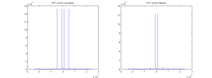
To help you test your fir31 module, we've written a Verilog test jig, fir31_test.v, which you can use with ModelSim to run your module through it's paces. When executed, the test jig reads the file fir31.samples, feeds them to your module, captures the output value and writes it to the fir31.output file. There are two sample files:
fir31.waveform which has 48,000 samples of a waveform constructed by adding together 1kHz and 5kHz sine waves. The expected outputs are given in fir31.filtered, which is approximately a 1kHz sine waveform. The frequency plots of fir31.waveform and fir31.filtered are shown below -- note how the 5kHz component has been filtered out!
To test your module, enter your design (and copy of the coeffs31 module from lab4.v) in a file called fir31.v. Then copy either fir31.impulse or fir31.waveform to fir31.samples, right-click on fir31_test.v and open with ModelSim, and issue the following commands:
vlib work
vlog fir31_test.v
When you get it to compile cleanly you can run the simulation with the folowing commands:
vsim fir31_test
run 1000ms
The simulation will stop after the last input sample has been processed. Now look at fir31.output to see what happened.
Step 3: Add the low-pass filter to your recorder module
In this step, add a single instance of the fir31 module to your recorder module. Use muxes to route data to the filter inputs, memory inputs, and to_ac97_data as described below.
The filter input to your recorder module is controlled by switch 0 on the labkit. When filter is 0, your recorder module should behave as before. When filter is 1 the fir31 module should be used as an anti-aliasing filter during recording and as a reconstruction filter during playback. Note that led[7] is on when filtering is enabled.
Here's a table showing the connections during various modes of operation:
| mode | filter | connections |
|---|---|---|
| record | off | filter_input = don't care mem_input = from_ac97_data to_ac97_data = mem_input |
| on | filter_input = from_ac97_data mem_input = filter_output[17:10] to_ac97_data = mem_input |
|
| playback | off | filter_input = don't care mem_input = don't care to_ac97_data = replicated mem_output |
| on | filter_input = zero-expanded mem_output mem_input = don't care to_ac97_data = filter_output[14:7] |
When the fir31 module is used as a reconstruction filter, it's input is a zero-expanded set of samples from the recording memory. "Zero expansion" is a type of up-sampling where one data sample is used from memory, followed by in our case seven samples of 0. The filter will interpolate between the memory samples, smoothly filling in values in place of the zeros. In this mode, the filter has a gain of 1/8 which we can compensate for by multiplying its output by 8. This is accomplished by simpling moving 3 bits to the right when selecting which output bits to use.
Which filtering operation seems to have the biggest effect: anti-aliasing or reconstruction? See the Implementation Tips below on how to use the logic analyzer to capture the playback data being sent to the AC97. During checkoff, show how the playback data changes when you switch the filter on and off.
Implementation Tips
After coding, examining the waveforms in simulation before attempting to program everything onto the FPGA can save you a lot of time. In particular, closely examine what happens when processing an incoming sample and generating a new outgoing sample (i.e., what your logic does on ready cycles). It's pretty easy to generate a known sequence of from_ac97_data values and ensure that they get written to your memory in record mode and get played back correctly in playback mode. Check that all control signals rise and fall as you would expect them to.
If your circuit seems to work under simulation but not when loaded into the labkit, try bringing critical signals out to the logic analyzer connectors, e.g., the signals for your 64Kx8 memory.
A good way to debug the filter is to use the logic analyzer to display your results. lab4.v includes code that outputs clock_27mhz to analyzer3_clock, to_ac97_data to analyzer3_data[7:0], and ready to analyzer3_data[8]. Configure the analyzer to sample the data on the rising edge of the clock if ready is 1. You can display the 8-bit data as a "magnitude waveform" in which the logic analyzer will plot the captured data values as a waveform. Zooming in, you should see the waveform as short straight line segments each made up of 8 points as your filter interpolator interpolates between the stored samples. There shouldn't be any big jumps between one captured value and the next if your filter is doing its job correctly.
In general, using the logic analyzer to examine what's happening is a quick way to "see inside" your chip and get some idea of what's going on.