Goal: Design, implement circuits using TTL logic; measure various circuit parameters using an oscilloscope and logic analyzer.
Useful links
Procedure
This lab is divided into several exercises to guide you through the design, construction, and debugging process. You will be asked to wire circuits for many of the exercises. Save all of these circuits until you have completed the lab as many of these circuits might be reused in subsequent parts of this lab.
Exercise 1: TTL/CMOS Static Electrical Characteristics
The logic values of 1 and 0 are represented by voltage levels in the hardware logic implementation. The voltage levels and other electrical characteristics are not standardized from one logic family to another. 6.111 will use both TTL (Transistor-Transistor Logic) and CMOS (Complementary Metal-Oxide Semiconductor) logic. The voltage ranges for the two logic families are not compatible.
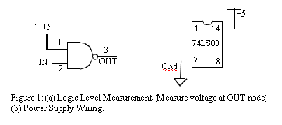
In this exercise, you will first measure the electrical characteristics of a TTL and CMOS gate using the circuit in Figure 1. Wire up this circuit using a 74LS00 part. Do not forget to wire power and ground! These connections are usually omitted from logic diagrams, as the power and ground of the 74LS series are generally the top-right and bottom-left pin, respectively. Typically, the top of the chip has a small semi-circular cutout, or a white dot next to pin 1.

Ground the input of the inverter (the first NAND) and measure the output voltage using the oscilloscope. Be sure to be using the voltage markers on the oscilloscope.
Now connect the input to a logic `1' and repeat the measurement.
Next, use a 74HC00 and wire up the same circuit and hook VCC to a +5V supply. Perform the same measurements and record your results.
Look up the valid input and output voltage ranges using the datasheet for a 74LS00 and a 74HC00. For each experiment, do your output values satisfy the range specified in the datasheets?
Consider interfacing a TTL inverter to a CMOS inverter and vice versa. Look at the datasheet titled "HCMOS Family Characteristics". Based on the +5V supply you used, find out the recommended input voltage for HCMOS inputs. Discuss potential issues when interfacing TTL and CMOS components? Run the two experiments (interface TTL to CMOS and vice versa) and make voltage measurements.
Exercise 2: Build Your Own Ring Oscillator
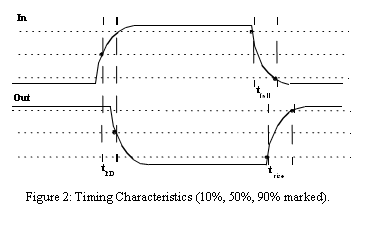
Important timing parameters associated with the speed of digital logic gates are the propagation delay time tPD, and the output signal rise and fall times, tR and tF. Propagation delay is a measure of how much time is required for a signal to change state. It is measured as the time from the 50% point of the input to the 50% point of the output (Figure 2). It is often cited as the average of the high-to-low and low-to-high delays (corresponding to the two transitions). The rise and fall times represent the amount of time for a signal to change state. To measure rise and fall times, you should be using the 10% to the 90% point, or vice versa.
Construct the ring oscillator shown in Figure 3 using a 74LS04 with as little wire as possible. From this circuit, determine the average propagation delay of a TTL inverter by measuring the period of oscillation by using the time markers on the oscilloscope. You can determine this by determining the number of gates a signal must travel through to complete a full period of oscillation.

What should the period of oscillation be with 3 inverters in the ring? Rewire the circuit and measure the period. Comment on the new result.
Insert a long piece of wire (about 3 feet) into the ring of 3 inverters. Observe how this extra length of circuit affects the signal. Can you explain the change?
Finally, take a single inverter and wire the output to the input. The voltage should be stable. If it isn't, connect a capacitor (0.01 uF) between this single node and ground to stabilize the voltage. Measure the voltage, and explain the significance of this voltage.
Exercise 3: Glitches
Wire up the circuit in Figure 4 using a 1.8432 MHz crystal oscillator and a 74LS00. Be sure to wire the crystal oscillator right side up. Pin 1 should be marked with a dot. The output GLITCH is a purposely glitchy output caused by the circuit. Using the oscilloscope, measure the width of the glitch.
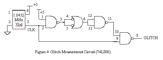
Next, add CLK and GLITCH as signals to the logic analyzer and measure the width of the glitch. Is there a significant difference between your two different types of measurements? Why does this glitch occur, and what is the lesson learned from this exercise? Under what conditions is it a bad idea to use a glitchy signal as an input?
Exercise 4: Asynchronous Counters
Wire up the 1.8432 MHz clock from the previous exercise to an 8-bit ripple counter as shown in Figure 5. You do not need to disconnect the previous circuit. In this exercise, we are concerned with how each output bit changes with respect to other bits. Since this counter increments its count every falling edge of the clock, each output bit must have a period twice that of the next significant bit. Because of this characteristic, counters make good clock dividers; if you want a slower frequency clock, it may be helpful to use a counter or a series of counters. Verify the counter's operation using the oscilloscope.
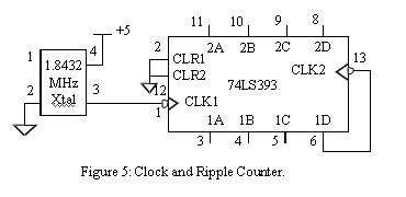
Trigger on either a rising or falling edge of the MSB, and measure the time between the falling-edge of CLK to edge of the MSB. Estimate the clk-to-q delay for each flip-flop in this chip.
Exercise 5: Synchronous Counter
One of the most useful of the 74LS series is the 74LS163. This is a 4-bit loadable synchronous counter with a synchronous reset. Wire two 74LS163s so that they count continuously as shown in Figure 6. The RCO output of the low-order counter is connected to the ENT input of the high-order counter. Explain when that signal is a 1 and how it controls the operation of the high-order counter.
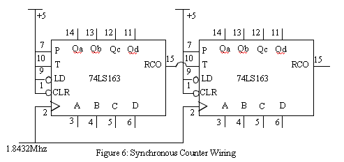
Using the oscillosope, measure the delay from the rising edge of the clock to when the QA output changes state. Do you get a noticeably different measurement for the QB output when it changes state? Explain.
Use the logic analyzer in internal timing mode ("timing acquisition") to capture the QA, QB, QC, QD and RCO outputs of the low-order counter. Display the values of QA, QB, QC and QD as a 4-bit hex number and trigger the analyzer so that it starts its display when the count is 0. Note that as the count changes from one value to the next, eg, from 0111 to 1000, it may momentarily read as other values depending on when one bit turns off and the other bit turns on. You can avoid these transitional values when triggering the logic analyzer by using an external clock to determine when values are sampled b the analyzer. Which signal and edge would we use if we wanted to sample the outputs of the couner?
It's possible for the RCO output to have momentary glitches after the rising edge of the clock. Explain the origin of these glitches.
Be prepared to comment on the difference between the 74LS163 and the 74LS393 in terms of design and performance; in particular, the speed and area of the device. By area, we are asking you to consider how complicated it is to implement the counter. How many flip-flops and how much logic is required to implement each counter?
Exercise 6: Designing Combinational Logic
In this exercise, you will be designing combinational logic that takes as input a 2-bit binary number and generates control signals that will properly illuminate a 7-segment display. Figure 7 shows the 4 possible digits.

Using Karnaugh Maps, design the combinational logic that converts the 2-bit input into control signals for each of the 7 segments of the display. Note that your logic should produce a "1" output in order to illuminate a segment. Fill out each Karnaugh Map, circle the terms in the Minimal Sum of Products and write the logic equation for each segment.
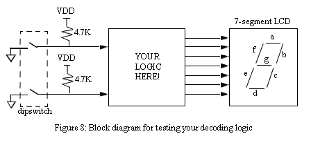
Draw a schematic diagram using only inverters and 2-input NAND gates that implements your logic equations. Construct the circuit on your protoboard using 74LS00s and 74LS04s (hint: you'll only need one of each IC) using a dipswitch to supply the 2-bit input as show in Figure 8. What's the propagation delay of your circuit?
