Goal: Build a voice recorder that records and plays back 8-bit digital audio samples.
Useful links
Checkoff List
Please be ready with the following when checking off Lab #4:
During checkoff you may be asked to discuss one or more of the following questions:
When you're done remember to upload your Verilog files to the course website so that they can be reviewed.
Digital Audio Interface
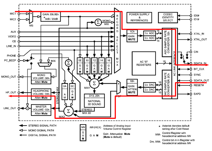
Our labkit is equipped with an AC97 Audio Codec chip (a National Semiconductor LM4550) which serves as an interface between the analog world of traditional audio components (e.g., headphones and microphones) and the digital world of the FPGA. The block diagram of the LM4550 shown below has been marked up to show the processing paths we'll be using for this lab:
Incoming audio from microphone (top arrow, pointing left-to-right): the incoming audio signal from the microphone is boosted by +20dB by an on-chip amplifier and then selected as the input source for the two (one for each of the stereo channels) 18-bit sigma- delta analog-to-digital converters (ΣΔADCs). The ADCs sample the analog waveforms at 48kHz, digitize the sampled voltages, and output sequences of 18-bit two's complement numbers (referred to as the pulse-code modulated or PCM data). Each pair (left and right channel) of PCM samples is packaged along with other status data into a 256-bit frame which is then transmitted serially at 12.288Mhz (= 256 * 48Khz) to the FPGA via the SDATA-IN pin.
Outgoing audio to headphones (bottom arrow, pointing right-to-left): the FPGA transmits a 256-bit frame of serial data to the AC97 chip via the SDATA-OUT pin. Each frame contains two 18-bit fields with PCM data for the left and right audio channels. The PCM data is converted to two 48kHz analog waveforms by the sigma-delta digital-to- analog converters (ΣΔDACs). The analog waveforms are amplified and sent to the stereo headphones.
So 48,000 times per second the AC97 codec provides two stereo PCM samples from the microphone and accepts two stereo PCM samples for the headphones. (Actually the microphone is a monaural source and so the same data appears on both the left and right incoming data streams.) It's the FPGA's job to keep up with the codec's data rates since the codec does not have on-chip buffering for either the incoming or outgoing data streams.
Voice recorder
The goal of this lab is to implement a voice recorder using the labkit's AC97 codec and FPGA. The top-level plan is pretty simple -- when recording, store the stream of incoming samples in a memory, when playing back feed the stored data stream back to the codec.
There are (of course) some interesting details:
Implementation steps
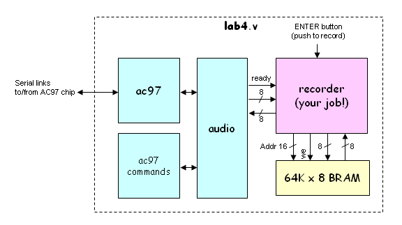
lab4: a modified version of labkit.v that includes instances of the audio and recorder modules, hooking them up appropriately to each other and the pins connecting to the AC97 codec. The labkit's ENTER pushbutton is used as the record/playback button (push to record). You shouldn't need to modify this module.
debounce: used to debounce and synchronize pushbuttons.
audio: a wrapper around the ac97 and ac97commands modules which implement the low-level interface to codec. This module has three ports of interest to us: a ready output that signals users of this module that a new sample is ready, and two 8-bit data ports, one for incoming monaural PCM data and one for outgoing monaural PCM data. You shouldn't need to modify this module.
ac97: interfaces with the AC97 codec, transmitting and receiving the 256-bit serial data streams. It has ports for both incoming and outgoing 18-bit stereo PCM data. You shouldn't need to modify this module.
ac97commands: generates a repeating sequence of writes to the AC97 command registers that perform the appropriate initialization. In this case, that includes selecting the microphone as the input source, setting the correct amplifier gains, etc. You shouldn't need to modify this module.
tone750hz: supplies a 20-bit PCM stream which if played at 48kHz produces a 750Hz sinewave. You shouldn't need to modify this module.
recorder: You'll be modifying this module to implement the necessary functionality. The supplied module tests the basic functionality of the microphone and headphones. In playback mode, this dummy module sends a 750Hz tone to the headphones. In record mode, it loops incoming samples back to the outgoing data stream, so you should hear your voice in the headphones. The module has the following ports all of which are synchronous with clock_27mhz:
| clock_27mhz | input | system clock |
| reset | input | 1 to reset the module to its initial state |
| playback | input | 1 for playback, 0 for record |
| ready | input | transitions from 0 to 1 when a new sample is available |
| from_ac97_data[7:0] | input | 8-bit PCM data from the microphone (signed, two's complement) |
| to_ac97_data[7:0] | output | 8-bit PCM data to the headphones (signed, two's complement) |
You can adjust the volume of the playback by pressing the UP and DOWN buttons (the top and bottom buttons in the diamond group of buttons to the left of the ENTER button). Each press will change the volume by 1 step over the range of 32 steps. During playback the current volume is displayed in the low-order 5 bits of the LEDs.
Record mode: When entering record mode, reset the memory address. When the ready input is asserted, a new sample from the microphone is available on the from_ac97_data[7:0] inputs at the rising edge of clock_27mhz. Store every eighth sample in the memory, incrementing the memory address after each write. You should also keep track of the highest memory address that's written. If you fill up memory, you should stop recording new samples.
Playback mode: When entering playback mode, reset the memory address. When the ready input is asserted, supply a 8-bit sample on the to_ac97_data[7:0] outputs and hold it there until the next sample is requested. For now, read a new sample from the memory every eight transitions of ready and send it to the AC97 eight times in a row (i.e., upsample the 6kHz samples to 48kHz using simple replication). When you reach the last stored sample (compare the memory address to the highest memory address written which you saved in record mode), reset the address to 0 and continue -- this will loop through the saved data again and again.
Test your code. If you have good ears you may hear a 6kHz tone (and its overtones) introduced by the simple upsampling by replication.
If the successive samples are S1 and S2 (S1 being the older of the two), then your module should output the following data over the course of 8 cycles of ready:
       S1             = (8 * S1) >> 3     (the right shift by 3 divides by 8)
.875 * S1 + .125 * S2 = (7 * S1 + S2) >> 3
.750 * S1 + .250 * S2 = (6 * S1 + 2 * S2) >> 3
.625 * S1 + .375 * S2 = (5 * S1 + 3 * S2) >> 3
.500 * S1 + .500 * S2 = (4 * S1 + 4 * S2) >> 3
.375 * S1 + .625 * S2 = (3 * S1 + 5 * S2) >> 3
.250 * S1 + .750 * S2 = (2 * S1 + 6 * S2) >> 3
.125 * S1 + .875 * S2 = (S1 + 7 * S2) >> 3
In general, on cycle i (for i from 0 to 7) you should output ((8-i)*S1 + i*S2) >> 3.
At this point S1 <= S2 and S2 <= new memory sample, and the whole process repeats for another eight cycles of ready.
NOTE: the samples from the AC97 are in 8-bit two's complement format, i.e., they range in value from -128 to +127. BUT the default Verilog data type is unsigned and multiplication circuits for unsigned operands are different than multiplication circuits for two's complement operands.
Using a feature introduced in the Verilog 2001 specification (which, happily, is supported by the Xilinx tools), you can solve this problem by adding a signed modifier to your register declarations so that Verilog knows that those quantities are in two's complement format, e.g.,
reg signed [7:0] s1, s2;
Now when, say, you use the "*" operator in your Verilog code, the Xilinx tools will generate the circuitry for signed multiplication instead of unsigned multiplication.
Implementation Tips
After coding, examining the waveforms in simulation before attempting to program everything onto the FPGA can save you a lot of time. In particular, closely examine what happens when processing an incoming sample and generating a new outgoing sample (i.e., what your logic does on ready cycles). It's pretty easy to generate a known sequence of from_ac97_data values and ensure that they get written to your memory in record mode and get played back correctly in playback mode. Check that all control signals rise and fall as you would expect them to. Another good time to use the simulator: examining the values produced by your linear interpolator -- you should see the appropriate intermediate values created over 8 ready cycles using two successive stored values.
If your circuit seems to work under simulation but not when loaded into the labkit, try bringing critical signals out to the logic analyzer connectors, e.g., the signals for your 64Kx8 memory.
A good way to debug the interpolator is to use the logic analyzer to display your results. lab4.v includes code that outputs clock_27mhz to analyzer2_clock, to_ac97_data to analyzer2_data[7:0], and ready to analyzer2_data[8]. Configure the analyzer to sample the data on the rising edge of the clock if ready is 1. You can display the 8-bit data as a "magnitude waveform" in which the logic analyzer will plot the captured data values as a waveform. Zooming in, you should see the waveform as short straight line segments each made up of 8 points as your linear interpolator interpolates between the stored samples. There shouldn't be any big jumps between one captured value and the next if your interpolator is doing its job correctly.
In general, using the logic analyzer to examine what's happening is a quick way to "see inside" your chip and get some idea of what's going on.